
- Controlled Orientation
- Fuel Cells
- Electric Fields
- Interfacial Interactions
- Solvent Induced Orientation
- Long-Range Ordering
- Solvent-Induced Ordering
- Salt Complexes
- Sheer Fields
- Droplet Evaporation
- Bulk Shearing
- Heterogeneous Surfaces
- Uniformly Modified Surfaces
- Heterogeneous Surfaces
- Chemical Heterogeneities
- Thermodynamics
- Entropy-Driven Transitions
- Closed-Loop Phase Behavior
- Super Critical Carbon Dioxide
- Salt Effects on Interactions
- Applications
- Templates for Pattern Transfer
- Scaffolds for Nanostructured Materials
- Nanowire Arrays
- Magnetic Storage
Solvent-Induced Orientation and Ordering
The self-assembly of materials is emerging as a key process in the fabrication of functional nanostructured materials, since it provides a powerful bottom-up route to well organized structures on the nanoscopic scale. Block copolymers, one class of self-assembling materials, offer an attractive route to fabricate nanometer-scale structures, since they spontaneously assemble a range of well-defined, well-ordered structures including spheres, cylinders, and lamellae, depending on the volume fractions of the components. In addition, the molecular weight of the copolymer provides control over the size and separation distances of the microdomains, and the specific functionality can be incorporated into the structure by varying the chemical nature of the copolymer.
This versatility makes block copolymers ideal candidates for use as templates and scaffolds for applications ranging from magnetic storage to displays and sensors. However, control of well-organized structures over a large scale is still challenging. For applications requiring addressability, long-range lateral order and orientation of elements are key, and therefore self-assembly is no longer sufficient. Rather, a directed self-assembly is required wherein the precise location of each nanoscopic element is defined. Normally this requires external fields, such as electric field, shear, temperature gradient, crystallization, chemically patterned substrate or controlled interfacial interactions. Very recently, we showed that solvent annealing and solvent evaporation at a controlled rate can provide a very simple but robust route to generating almost defect-free microstructures over large areas in block copolymer thin films.
Generating laterally ordered, ultradense, macroscopic arrays of nanoscopic elements will revolutionize the microelectronic and storage industries. We use faceted surfaces of commercially available sapphire wafers to guide the self-assembly of block copolymer microdomains into oriented arrays, with quasi-long-range crystalline order over arbitrarily large wafer surfaces. Ordered arrays of 3 nm diameter cylindrical microdomains, with areal densities in excess of 10 Terabit/inch2, have been produced. The saw-toothed substrate topography provides directional guidance to the self-assembly of the block copolymer, which is tolerant of surface defects, like dislocations. The lateral ordering and lattice orientation of the single-grain arrays of microdomains is maintained over the entire surface. This approach is parallel, applicable to different substrates and block copolymers, and opens a versatile route toward ultrahigh density systems.
We also demonstrated a simple, versatile approach to the directed self-assembly of block copolymers into a macroscopic array of unidirectionally aligned cylindrical microdomains on reconstructed faceted single crystal surfaces or on flexible, inexpensive polymeric replicas. High fidelity transfer of the line pattern generated from the microdomains to a master mold is also shown. Single-grained line patterns over arbitrarily large surface areas without the use of top-down techniques is demonstrated, which typically have an order parameter typically in excess of 0.97 and a slope error of 1.1o. This degree of perfection, produced in a short time period, is yet to be achieved by any other method. The exceptional alignment arises from entropic penalties of chain packing in the facets, coupled with the bending modulus of the cylindrical microdomains. This is shown, theoretically, to be the lowest energy state. The atomic crystalline ordering of the substrate is transferred, over multiple length scales, to the block copolymer microdomains, opening avenues to large-scale roll-to-roll-type and nanoimprint processing of perfectly patterned surfaces, and as templates and scaffolds for magnetic storage media, polarizing devices, and nanowire arrays.
Solvent evaporation is a strong, highly directional field. Strong repulsion between the copolymer blocks, combined with the directionality of solvent evaporation, where ordering is initiated at the surface of the film and propagates through the entire film, leads to a high degree of long range order with few defects. Studies were performed on a polystyrene-block-poly(ethylene oxide) copolymer (PS-b-PEO), where the minor component is the PEO. After spin coating, cylindrical structures were generated normal to the surface, having poor lateral order. After some thermal annealing, the order improves such that micron size grains can be observed after 96 hours. However, the use of solvent annealing with controlled evaporation was found to be superior to thermal routes in the ordering of the copolymer. The solvent imparts a high degree of mobility in the microphase-separated copolymer, enabling a rapid removal of defects and, a high degree of lateral order.
In situ grazing-incidence small-angle x-ray scattering experiments on thin films of block copolymers of polystyrene-block-poly(2-vinylpyridine) (PS-b-P2VP) during annealing in neutral solvent vapors are reported. By removing the solvent in a controlled manner, the period of the microphase separated morphology is found to increase, with increasing block copolymer concentration, in a power law manner with an exponent of 2/3. By venting the systems at different rates during the solvent removal process, kinetically arresting the system, the period of the microphase separated morphology in the dried film can be varied.
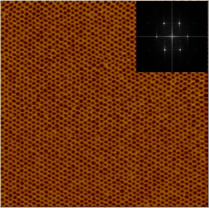
Figure 1. SFM phase image of PE-PEO thin films after annealing for 48h in a benzene vapor under controlled humidity.
|
Even with solvent evaporation and solvent annealing techniques, it is difficult to achieve grain sizes that are greater than tens of microns. Generally, there is no preferential macroscopic grain orientation and limited translational order. However, it has been shown that by using a patterned substrate that has features on the order of microns, such as parallel lines etched in an oxide layer, one can achieve improved lateral order. We have been able to use this to provide a preferential macroscopic grain orientation where the grain orientation is defined on large length scales. A solution of PS-PEO was spin coated onto a silicon oxide surface containing channels 875 nm wide and 325 nm deep. The same solvent annealing strategy was applied. As can be seen in Figure 2, an essentially defect-free array of cylindrical domains oriented normal to the surface is obtained within each channel. This order propagates along the length of the channels over hundreds of micrometers.
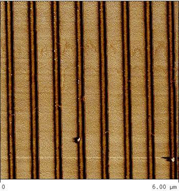 |
Figure 2. SFM image of PS-PEO on a topographically patterned surface
|
We recently uncovered a unique means of inducing a robust orientation of microdomains in PS-b-PEO, by the use of a wide variety of salts. In particular, by incorporating dilute concentrations (1%) of M+X- , where M can be K, Li or Cs and X can be Cl or I, into the solution used to prepare the thin PS-b-PEO films, a pronounced orientation of the cylindrical PEO microdomains, with lateral long range order after solvent annealing, was observed. Unlike the preparation of the pure PS-b-PEO films, which are extremely sensitive to changes in the humidity, the addition of the salt resulted in humidity having very little, if any, influence on the orientation of the microdomains. More recently, we show that by placing a cleavable juncture, a triphenylmethyl (trityl) ether linkage, between PS and PEO, highly ordered nanoporous thin films could be prepared directly from PS-b-PEO diblock copolymers. Combining the above two strategies, a cleavable PS-PEO complexed with salt was prepared, and used for generating thin films with lateral long range order on a topographically patterned surface. As seen in Figure 3, a highly ordered nanoporous thin film can be readily generated.
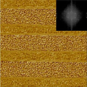 |
Figure 3. SFM phase image of cleavable PS-PEO with slat on topographically patterned surface.
|
Electric Fields Controlled Orientation and Templates for Nanostructured Materials
Block copolymers (BCPs) are emerging as promising candidates as scaffolds and templates for the fabrication of nanoscopic structures. Key to the use of block copolymers is the control of the lateral ordering and orientation of the microdomains in BCP thin films. Electric field is proved to be able to orient the microdomains either in the plane of the substrate or perpendicular to it. For in-plane alignment of BCPs, electrodes need to be fabricated by standard optical lithography and electron-beam evaporation of a metal. Initially, the axes of the cylinders are lying parallel to the substrate due to surface interactions. The axes can then be induced to stretch along the electric field lines when film is simultaneously heated above the glass transition temperature of both blocks. Since electric fields with an order 30 kV/cm were necessary to orient the domains, the patterning of an entire wafer would require the use of multiple electrodes and a careful understanding of the electric field formed when applying a voltage between electrodes on top of a thin insulating layer on a conducting substrate. When an external eclectic field is applied to across the film, PMMA cylinders in PS metric can be oriented perpendicular to the substrate and these ordered arrays can be used to grow nanowires either by electrodepositing through the porous template or by using it as a mask for etching or patterning the underlying substrate, as schematically illustrated in Figure 4. Analysis of scattering patterns indicated that during alignment of the lamellar microdomains, the material goes through an intermediate state with substantially reduced long-range order. After orientation, the sample consists of many small grains with the lamellae being oriented parallel to the electric field and a random orientation in the plane perpendicular to the field.
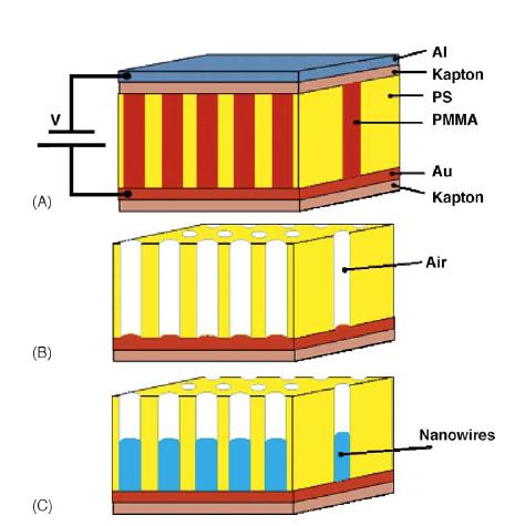
Figure 4. Schematic representation of high density nanowire fabrication in a polymer matrix. (A) An asymmetric diblock copolymer annealed above the glass transition temperature of the copolymer between two electrodes under an applied electric field, forming a hexagonal array of cylinders oriented normal to the film surface. (B) After removal of the minor component, a nanoporous film is formed. (C) By electro-deposition, nanowires can be grown in the porous template, forming an array of nanowires in a polymer matrix.
|
Furthermore, our most recent results show that lithium ions coordinate with the carbonyl groups in PMMA block to form lithium-PMMA complexes, resulting in a significant increase of the Flory-Huggins segmental interaction parameter, as well as dielectric contrast between PS and PMMA blocks. The increased segmental-segmental interaction parameter X drives PS-b-PMMA block copolymer from a weak segregation regime into a strong segregation regime. Thus the local order of the microdomains was markedly enhanced both in bulk and in films without applying any external fields. The increased dielectric contrast significantly amplified the driving force to align the BCP microdomains in films under an external electric field and reduced the critical electric field strength required to overcome the preferential interactions of the blocks with the substrate. Therefore, the complete alignment of lamellar microdomains in PS-b-PMMA block copolymer thin films has been achieved by using an electric field (Figure 5).
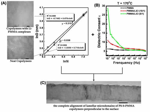
Figure 5. (A) Left: TEM images of PS-b-PMMA and PS-b-PMMA with lithium complexes after annealing at 170 °C for 2 days (no electric field was applied) followed by quenching to room temperature. Right: Domain spacing, D, vs chain length, N, in a double-logarithmic plot. Triangle: data from PS-b-PMMA copolymers; diamond: data from corresponding PS-b-PMMA copolymers with lithium complexes. Full lines: nonlinear least-squares fitting with an R2 of 0.999 for each line in the range N = 535-1102. (B) Dielectric constants of PMMA with different molar ratios of added LiCl to the carbonyl group 0 (black), 1:10 (red), and 1:6 (green) at 170 °C. (C) Cross-sectional TEM image of PS-b-PMMA thin film with almost saturated lithium-PMMA complexes after annealing at 175±5 °C in N2 environment under a dc electric field of ~ 40 V/mm for 24 h.
|